Panaxis FMX PLL FM Exciter Review
First Impressions
This review unit was borrowed from a third party, who had constructed it from a kit.
It costs $120.00 (kit). This unit is mono, for stereo it must be used in
conjunction with a stereo encoder. Thirteen pages of
documentation are provided. These cover:
- Introduction, specification, legal warning
- Theory of operation (oscillator and amplifier; PLL operation; modulation; ALC circuit;
power supply)
- Enclosure options
- Audio circuit options
- RF circuit options
- Operation and testing (frequency selection; PLL range; output tuning; audio connections)
- Parts List
- Assembly instructions
- PCB diagram
- Schematic
 The documentation is comprehensive and well written, and explains the various
audio, RF and power supply options available on this unit. The high quality double
sided printed circuit board has a component placement silk screen on the top side, and top
and bottom solder resists which assist in making good solder joints.
The documentation is comprehensive and well written, and explains the various
audio, RF and power supply options available on this unit. The high quality double
sided printed circuit board has a component placement silk screen on the top side, and top
and bottom solder resists which assist in making good solder joints.
The frequency is set by 3 miniature BCD (binary coded decimal) switches, using a small
screwdriver. The switches are mapped to 10s, 1s and 0.1s of MHz, making frequency
selection straightforward. External thumbwheel switches can be fitted as an alternative.
Two LEDs indicate loop lock and ALC (automatic level control) activity.
The only tuning required for this kit is to set the centre frequency of the VCO tank
coil. Various correspondents have reported that this is difficult to achieve without
breaking the fragile ferrite core. An appropriate plastic trimming tool (not
supplied) should be used for this purpose. Another variable inductor is used in the
RF output low pass filter (LPF). This is supplied ready adjusted. A ceramic
trimmer sets the centre frequency of the 4MHz frequency oscillator. If a frequency
counter is not available, this can be left in its centre position (half moon top electrode
rotated 180° from the flat on the trimmer body).
The schematic and parts list for this unit are available at
www.geocities.com/Area51/Nebula/3736/
(archive.org).
Circuit Description
The transmitter uses the standard PLL architecture.
The voltage controlled oscillator (VCO) is based on a
2N5109 NPN bipolar transistor and operates at the output frequency. The
centre frequency of the VCO is set by an adjustable inductor, which forms a tank circuit
with a MV104G dual varicap diode. This varicap is used as both the audio
modulator, and the VCO control element, as it is connected to the DC output of the PLL
loop filter. This DC feedback path enables the output frequency to be locked to the
frequency of a stable crystal reference oscillator. The audio input circuit is totally
passive, though there is an unorthodox ALC (automatic level control) arrangement based on
a pair of diodes. Pre-emphasis
is provided by a parallel resistor/capacitor network in the audio input path. The
supplied resistor is for USA/Japan 75uS pre-emphasis, it must be changed for European 50uS
pre-emphasis. If the unit is to be used with a stereo
encoder, a different input is used which bypasses the pre-emphasis and ALC circuits.
The output of the VCO is coupled by a resistive T attenuator straight to the output
stage. This design is unusual in not having any intermediate buffering/gain stage
between the VCO and output stage, which also means the VCO is operating at a power higher
than usual for low noise VCOs. A sample of the VCO output is also passed to the fin
input of the synthesiser IC. The output transistor is another 2N5109, fitted with a
small aluminium heatsink. This device is not designed for power, and I'd be
extremely sceptical that you could get any where near to the quoted 0.5W output power.
A three section pi low pass filter (LPF) and another resistive T attenuator (not
fitted in review unit) complete the RF path. The variable inductor in the LPF is
supplied pre-tuned. There is provision to fit a type "F" RF output socket.
There are three possibilities to select different levels of output power:
- The output device is powered from the +6V rail [jumper "LPJ"]
- The output device is powered from the unregulated side of the +6V regulator (after the
on-board bridge rectifier and a 22R resistor [jumper "HPJ"])
- The output device is powered directly from an external regulated power supply (apply
power to the top of the 22R resistor R18 [shown as 10R on schematic at
www.geocities.com/Area51/Nebula/3736/)
The review measurements were performed with option 2. The instructions state that
for extra power the output device bias resistor can be reduced from 4.7K to 3.3K, for a
nominal 200mW output. This was not tried. 200mW is a long way from the 500mW
mentioned on the page 1 of the supplied instructions.
The PLL is implemented with the popular Motorola MC145170 PLL frequency synthesiser
IC (MC145170
data sheet (PDF format) - 382Kb). This synth chip has a three
wire serial interface, consisting of data in, clock and enable. The frequency
reference comes from a 4MHz crystal, trimmed by a variable capacitor. The loop
reference signal is 100KHz, as became evident during the RF tests, as it's all
over the RF output signal. The supply is this IC is +6V, which is interesting,
as the manufacturers data sheet clearly states that the maximum input voltage
rating for this part is +5.5V. Now the part obviously works at this voltage
- but for how long? Will it last 3 months? A year? 3 years? Who
can say? This is certainly not normal practice and constitutes bad design
in my book. Presumably this decision was taken to extend the range of
the VCO control voltage to cover 20MHz without having to retune the VCO tank
inductor. The way this is done properly is to use an external active loop
filter, running off a higher supply voltage, as implemented in, for example,
the Broadcast Warehouse 1W FM LCD PLL Exciter.
The synth chip drives an on-board lock detect LED via a 2N3904 transistor, and is
also fed into the PIC to detect loss of lock. The loop filter is passive. As
the supply rail to the synth chip is +6V, this limits the useful range of the VCO control
voltage to about 5V. To tune across nearly 20MHz with 5V requires the VCO tank coil
to be set quite precisely.
The synth chip is programmed by a Microchip
Technology PIC16C52 8 bit microcontroller, running off its internal clock. This
chip is one time programmable, and presumably runs code written by Panaxis. Programming information is derived from
a 3 BCD switches. This allows the frequency to be set in 100KHz steps, in the range
87.9MHz to 107.9MHz. This is slightly unfortunate, as the FM broadcast band extends
from 87.5MHz to 108MHz.
The FMX has two synth programming mode, "test" and "reset".
In "test" the synth is programmed every couple of seconds. In
"reset" it appears that the synth is programmed on power-up or if lock is lost
for any reason. In "reset" mode the BCD switches are not scanned (apart
from power-up or lost of lock), so "test" mode is used to change frequency.
The unit should not be operated on air in test mode, as the synth programming can
be heard as a "ticking" on the audio; on a spectrum analyser the RF can be seen
to momentarily shift frequency as the synth is programmed.
This "test" and "reset" mode business strikes me as unnecessarily
complicated. I don't see why the PIC couldn't just scan the BCD switches and
reprogram the synth when a change is detected, as the Broadcast Warehouse 1W PLL
Transmitter does. The review unit could not be persuaded to come out of
"test" mode. I forced it into "reset" mode whilst taking
spectrum analyser plots by removing the J1 jumper and applying +6V to the centre pin of
J1.
A small voltage regulator provides a stabilised +6V supply to the whole circuit apart
from the RF output device.
Construction
The double sided printed circuit board (PCB) supplied has plated through
holes, making the removal of a wrongly placed component difficult, so extra care is
required when fitting the components As the components are closely spaced to one
another, a small bit on the soldering iron is
essential. Any potential constructors new to soldering are advised to practice on a
scrap PCB with some cheap unwanted components before moving on to the real thing.
The instructions should be scrutinised carefully to identify which of the
many options are desired. Panaxis helpfully suggests that the desired sections
should be marked with a high-lighter pen. Three hours is suggested as a typical
construction time.
Test Results
The loop locks within a couple of seconds, this is indicated by the loop
lock LED glowing brightly.
Frequency Response and Output Power
With a 16V supply, the output power and VCO control voltage were accurately measured
and plotted below. +16V to the input of the on-board bridge rectifier results in
+14.5V on the jumper J2, and +12.4V on the collector choke of the RF output device.
The supply current varied from 110mA at 87.9MHz to 96mA at 107.9MHz.
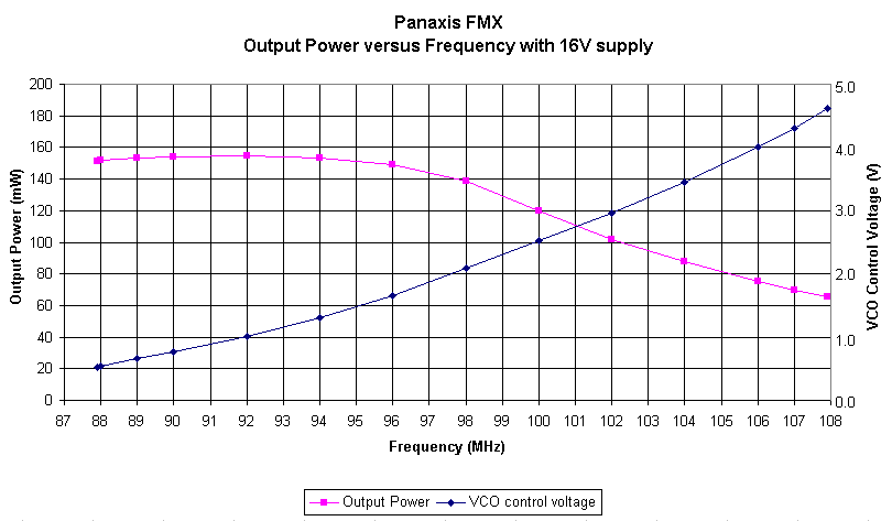
As can be seen from the graph, the output power remains steady at 150mW to about 96MHz,
it then tails away to 65mW at the top end of the band. This disappointing 3dB power
over frequency variation makes this unit difficult to use with a wideband (no-tune) power
amplifier. The plot of the VCO control voltage, taken from the output of the loop
filter (top of R7), demonstrates that the VCO control voltage is properly positioned
within its valid range. If at the extremes of the frequency band, this voltage
became too high (say above 5.5V) or too low (say below 0.5V), the loop would be in danger
of losing lock with variations over time and temperature, or under high audio modulation.
The graph also shows how critical this adjustment is, with little margin in error
in setting this centre frequency. The slope of the control voltage plot gives the
tuning sensitivity of the VCO as approximately 5MHz/V.
Output Power versus Supply Voltage
The frequency was set to 98MHz. The table below shows the supply current and
output power as the supply voltage was reduced from 16V.
Supply
Voltage (Volts) |
Supply Current (mA) |
Output Power (mW) |
| 16 |
105 |
140 |
| 15 |
100 |
126 |
| 14 |
96 |
112 |
| 13 |
93 |
98 |
| 12 |
88 |
86 |
| 11 |
81 |
70 |
| 10 |
67 |
45 |
| 9 |
52 |
24 |
| 8 |
37 |
10 |
| 7 |
23 |
3 |
| 6 |
12 |
0.2 |
The unit lost lock at +6V supply, by which time the RF output power was effectively
zero. The DC to RF efficiency of the FMX is not good, considering the Broadcast Warehouse 1W LCD PLL Transmitter puts out over 5
times the output power (800mW nominal at +13.8V supply) for twice the supply current. The
small current drain of this unit makes battery operation a possibility, though for some
applications the output power is a bit weedy.
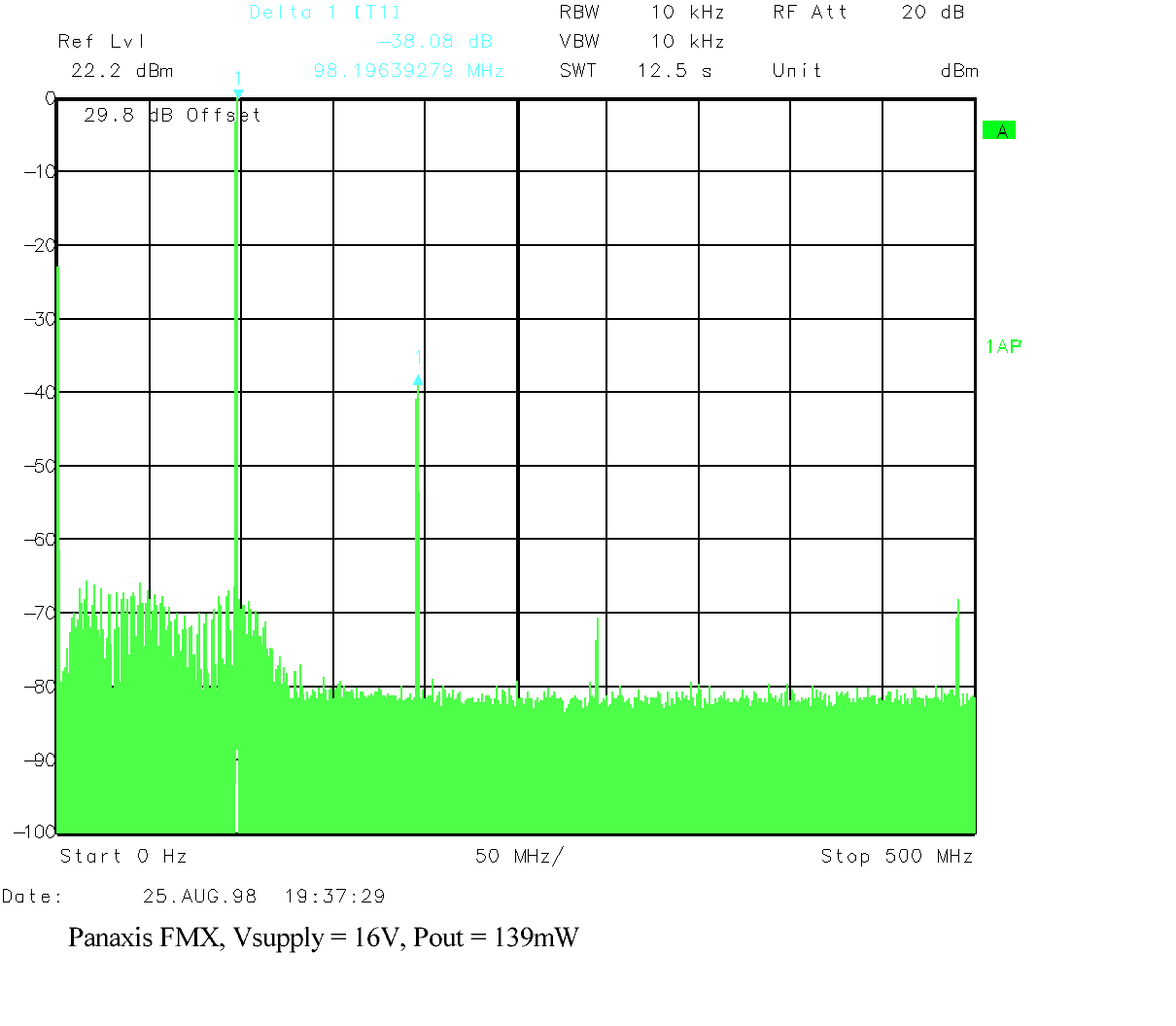
At +16V supply, the harmonics were measured on a
spectrum analyser at 88, 98 and 108MHz centre frequencies.
As can be seen from the table and the spectrum analyser plots, the worst harmonic,
-31dBc at 88MHz is considerably worse than the -40dBc specification figure. It could
be argued that the harmonics could be optimised for a particular frequency by adjusting
the LPF variable inductor. But this requires use of a spectrum analyser, which the
vast majority of potential customers will not have access to. Far preferable to
implement a LPF which guarantees minimum harmonic rejection without adjustment.
Apart from that, the harmonics are not too bad, and given the units small output power, it
could be connected directly to an aerial.
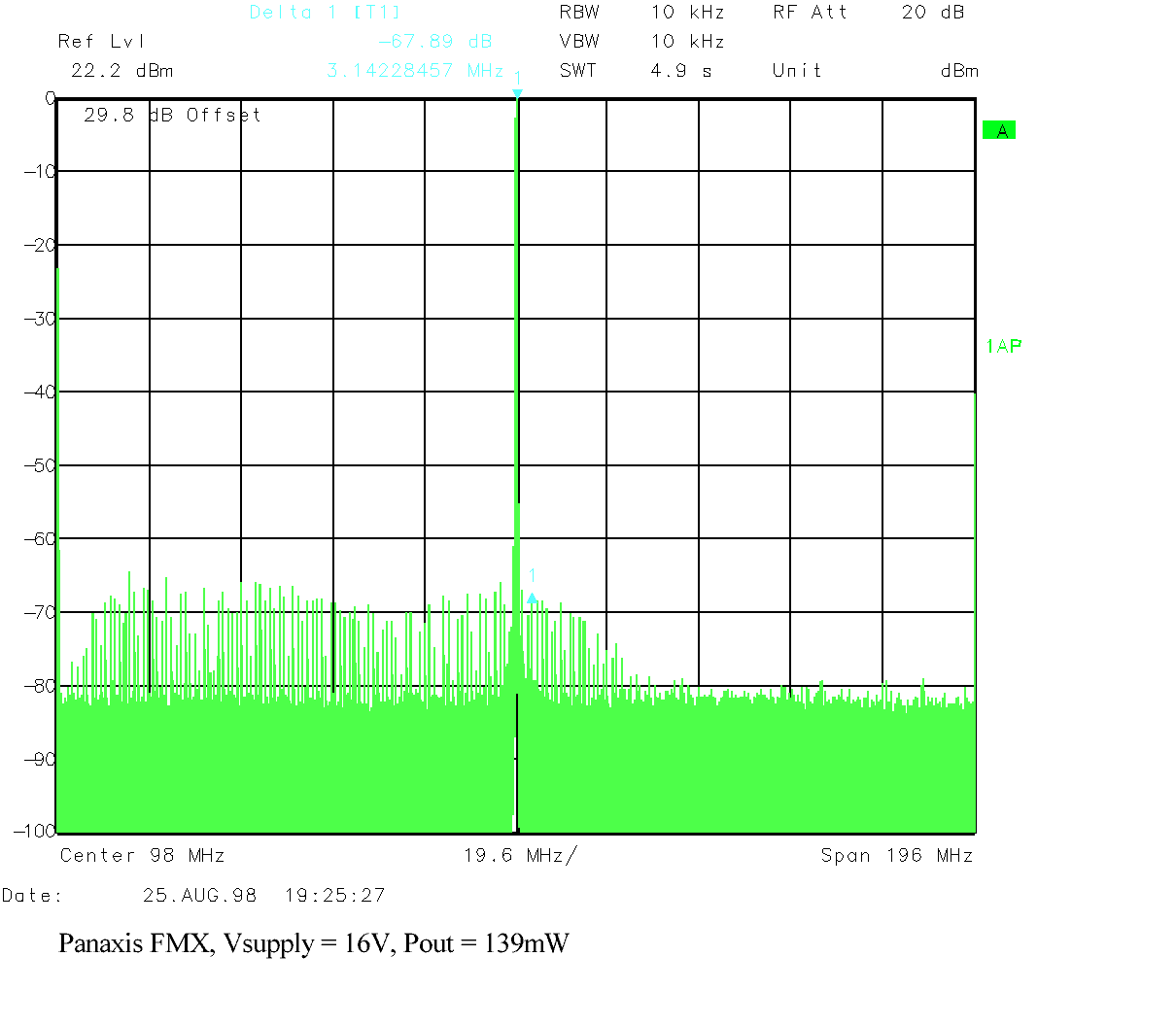
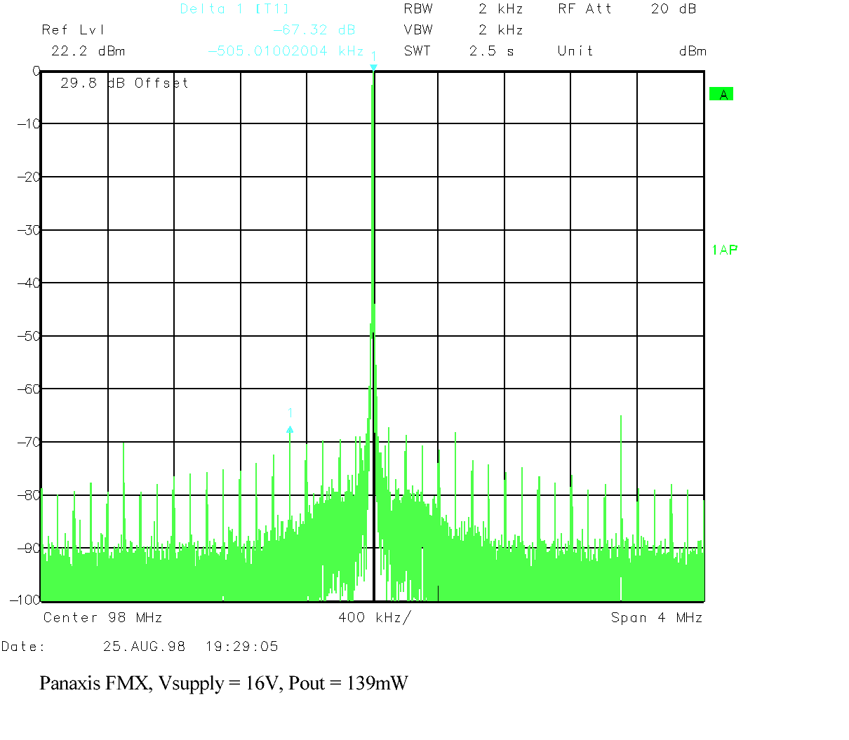
The spurious performance is not particularly satisfactory, with a veritable forest of
100KHz spurs extending right down to 10MHz. These spurious components are not
particularly high level, -67dBc at -500KHz offset for example, but as other manufacturers
have achieved far better performance using very similar components, the inevitable
conclusion is that with a little more care in design and lay-out, this unit could have
been easily yielded much better specifications.
Mismatch Tolerance, Audio Response
Due to the small output power capability of the unit, bad VSWRs are unlikely to damage
this unit, especially if the output T attenuator is fitted. Audio response has not
measured - yet. Other correspondents have reported poor low frequency audio
response. This will be the subject of further work.
Conclusion
Good construction plans, ease of tuning and a quality PCB and components
are let down by bad design (over running synth chip, poor spurious rejection).
Furthermore the small output power, especially at the top of the band, and reputed poor
audio response lead me to the conclusion that your money is better spent elsewhere.
Not recommended.
Review Revision History
The construction plans are titled "FMX (rev. 1)". The PCB is marked
"WPC-Z".
RF measurements were made 25 August 1998. This review was prepared 1 September 1998.
FMX1 Spectral Output - by
David Schmidt (measured on Dec 5, 1996) from archive.org
[ How to be a Community Radio Station Home
Page | Introduction to Community Radio Station Electronics
]
Other Reviews
Thanks to Web Surf from FM
Transmitter Kits, RF Circuits, Schematics, Exciters .... for his help in formatting tables.
Last updated 23 August 2003